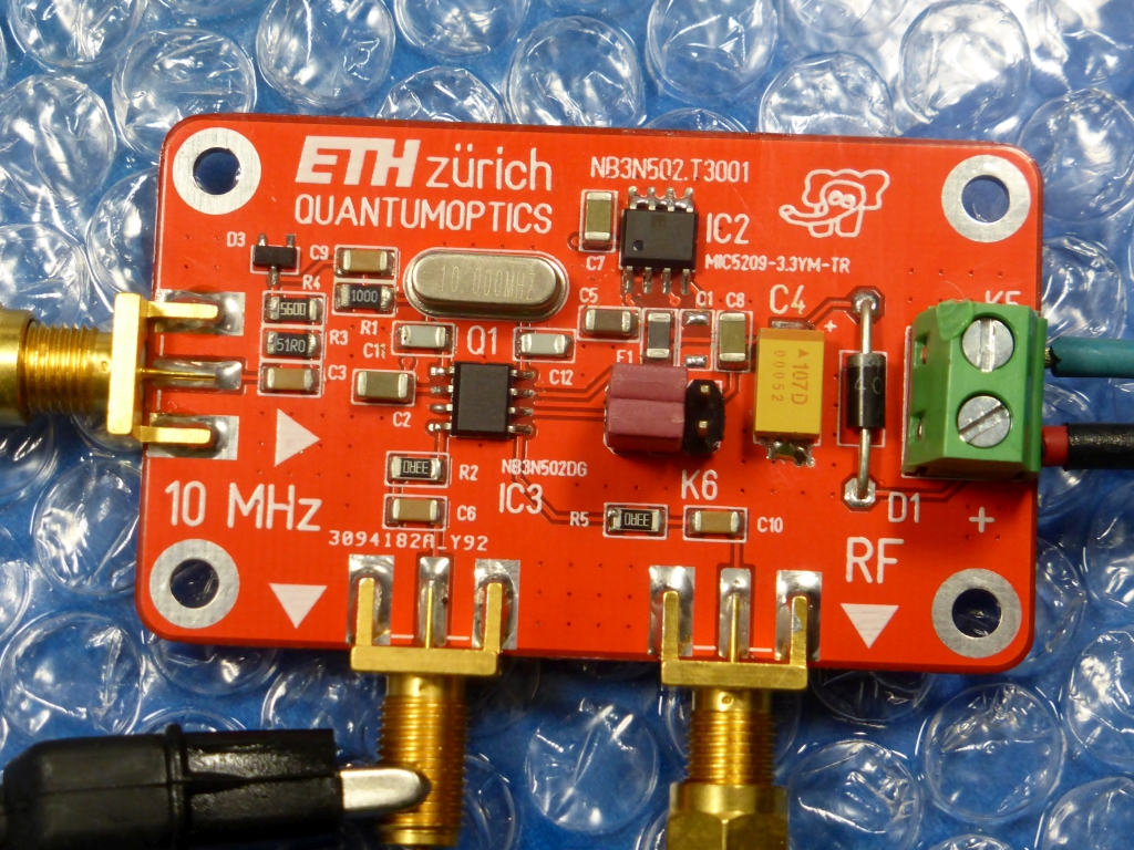
A versatile Reference Clock Source with the NB3N502
THE PROTOTYPE
✈ Motivation
In a Lab, a lot of devices need clocks. And they must all be locked to a 10 MHz Reference.
At the same time, they still must produce a useful output, in case those 10 MHz are
not available (in case the device is taken to the office for software development e.a.).
✈ Circuit Description
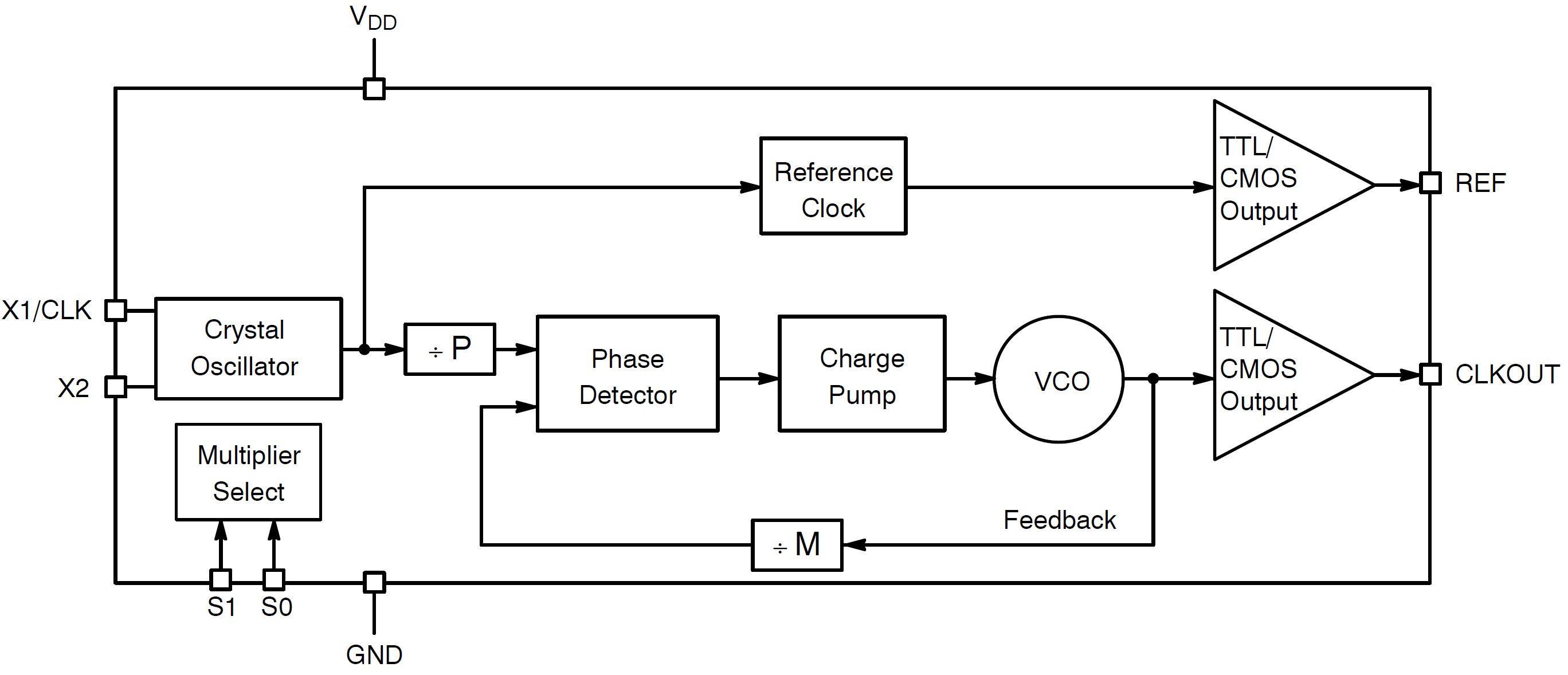
Block Diagram of the NB3N502 - Drawing Courtesy of ON Semiconductor
Starting at the left side, the chip contains a crystal oscillator. This is build around an
inverter circuit, which has a feedback resistor (internal) to bring the inverter gate into a linear operation.
Application Note 118
from Fairchild Semiconductor (1974) mayst be helpful to understand this circuit in detail. This
oscillator is equipped with a 10 MHz fundamental crystal. It does oscillate and therefore supplies
the PLL circuit with a stable Reference.
In case we connect another 10 MHz Source (external), the feedback fom the crystal is overdriven
and the inverter gate acts as a Buffer-Amplifier. A Diode Network (BAV99) limits the amplitude of an
external Signal to approx. 1.4 Vpp. A series-resistor as well as a coupling capacitor
ensure a very light coupling and also act as a dc-block. It shall avoid, that if a coaxial cable
(with no Reference) shall load the oscillator cicuit too much, so that oscillation could stop.
Following the Reference Oscillator/Buffer is a VCO/PLL equipped with a Reference Divider and a Feedback
Divider. The VCO consists of a differential voltage controlled ring oscillator design using NMOS gate
oxide capacitors in the loop filter to provide lowest leakage.
The Division ratios can be set via two jumpers, which are connected to the S0/S1 inputs
of the Chip. It shall be noted, that those two inputs have three valid voltage Ranges. If no Jumper
is set, Pin S1 defaults to M and Pin S0 defaults to H. M in this case is something like
"middle" as an internal voltage divider pulls this input to approx. 1.65 V
when powered by a 3.3 V source.
When used with a 10 MHz input signal, a maximum output frequency of 50 MHz is obtainable. For
higher frequencies at the input, a maximum output frequency of 120 MHz is the limit. By design.
The supply voltage is stabilised by a MIC5209 from Microchip Technology Inc. It's datasheet says :
"Key features include reversed-battery protection, current limiting, overtemperature shutdown,
ultra-low-noise capability". It turned out, that this is a nasty little thing. If your
bypass capacitors are too good, it will oscillate !
Possible Multiplication Factors :
MULTIPLICATION
JUMPER S1
JUMPER S0
2.00 X
GND
GND
2.50 X
VCC
VCC
3.00 X
OPEN
GND
3.33 X
OPEN
VCC
4.00 X
VCC
GND
5.00 X
GND
VCC
✈ Downloads
✈ Performance
Even so, the datasheet of the NB3N502 mentions only "typically" values for the Jitter,
we know from a trustworthy source, that the worst case jitter occurs when using a 6 MHz crystal.
Using a 16 MHz or 26 MHz crystal, the rms jitter is well below 15 ps. And it looks like it goes down
when the multiplication factor goes up.
Symbol
Characteristic
Min
Typ
Max
Unit
tjitter
Period Jitter (RMS, 1 σ)
15
ps
tjitter
Total Period Jitter, (peak−to−peak)
±40
ps
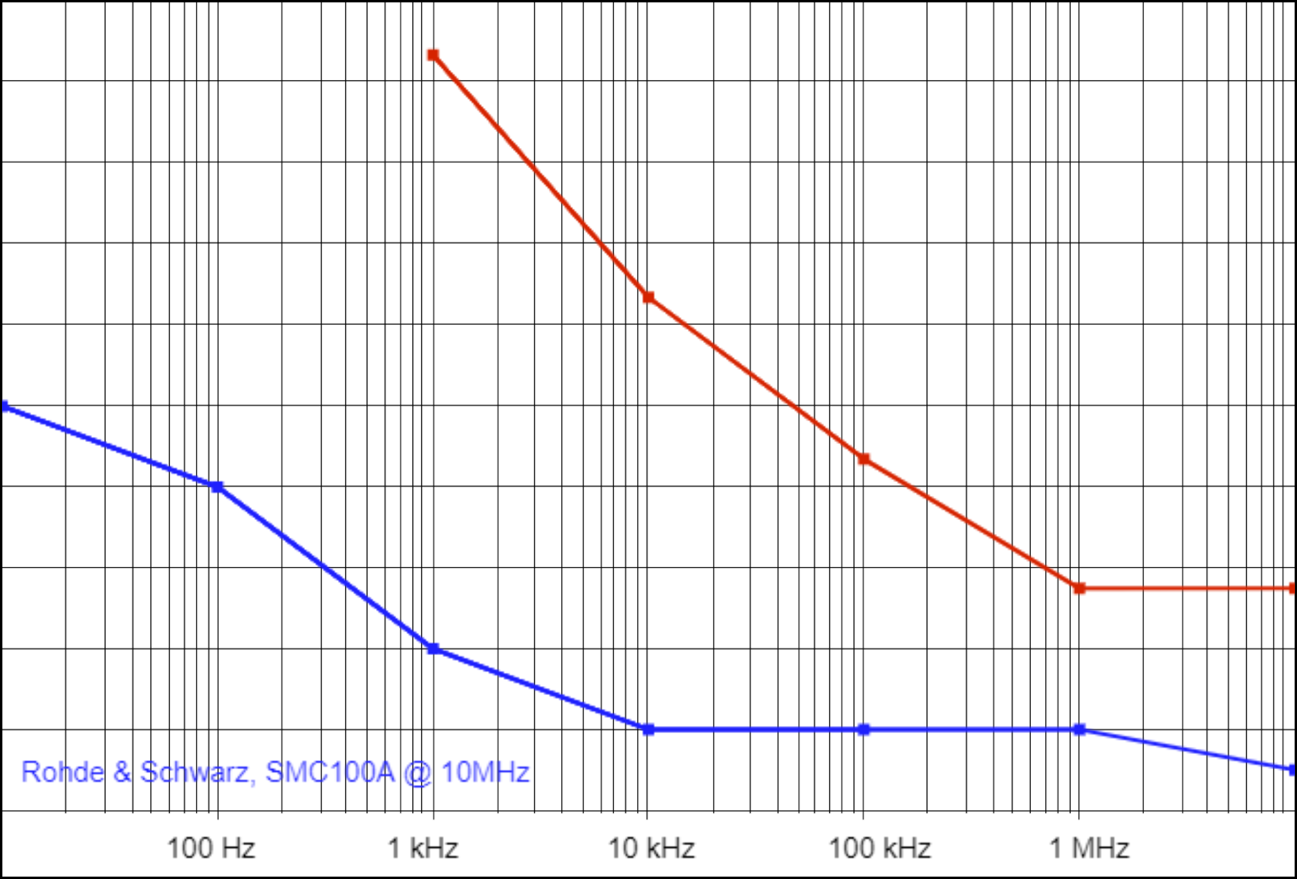
From that, we would expect a Phase Noise somewhere near that pictured below (left). And
yes, we used
this nice tool to create the graph. We made the following assumptions : VCO is like an LC-oscillator.
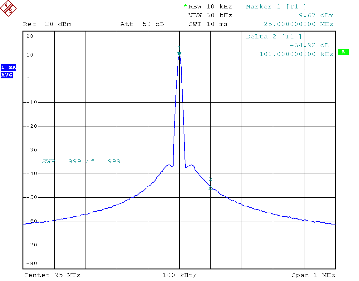
Jitter was measured at 25 MHz. Top level -60 dBm, 10 dB/DIV.
Comparing the 'Guesswork' with the 'Real Life' :
Sophisticated Guess (compared to a R&S)Measurement: ext. 10 MHz in, 25 MHz out
The Cursor readings are : 25 MHz .:. + 9.67 dBm, 25.1 MHz .:. - 54.92 dBm. RBW was 10 kHz. To normalise
the offset reading to 1 Hz, we have to subtract 10 * LOG(10 kHz) = 40. This will then give us
- 94.92 dBm/Hz. Setting this in relation to the carrier, we get - 104.59 dBc/Hz @ 100 kHz Offset.
✈ Other Applications
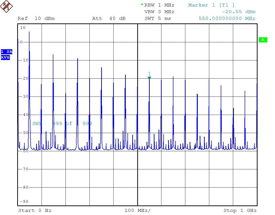
Due to the digital nature of this thing, a lot of harmonics are generated. Depending on the
multiplication factor, the phase comparator frequency and or the input frequency is visible
more or less close to the carrier. So frequency planning is a must, when this is your application !
✈ Share your thoughts
The webmaster does not read these comments regularely. Urgent questions should be send via email.
Ads or links to completely uncorrelated things will be removed.
 ช้างเผือก