 ช้างเผือก
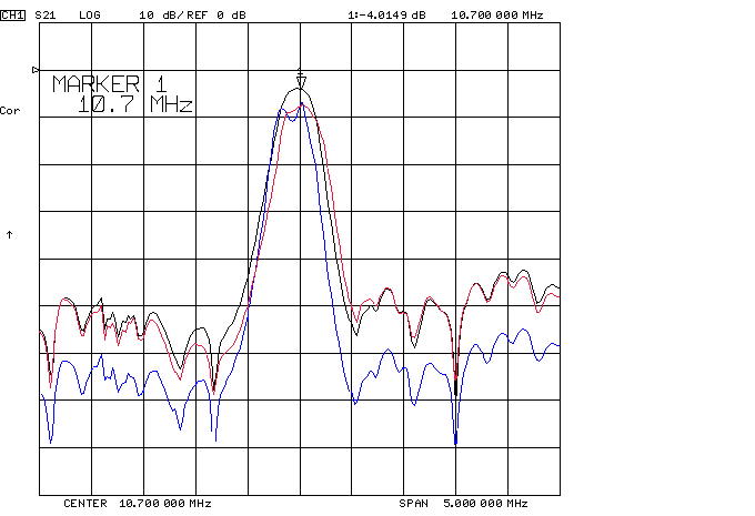
Categories
Statistics
Since 08.08.2014
Counts only, if "DNT = disabled".
216.73.216.253
216.73.216.253
Counts only, if "DNT = disabled".
216.73.216.253
216.73.216.253
Info

เราจะทำแบบวิศวกรผู้ยิ่งใหญ่
27. July 2026
YOUR OPINION •••
average: 0.001, n: 0

When using this form, your ip is stored in order to avoid multiple voting on the same website. That's it.
When using this form, your ip is stored in order to avoid multiple voting on the same website. That's it.
ceramic_bandpass_filter.php 15559 Bytes 04-03-2025 19:12:07
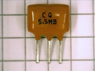
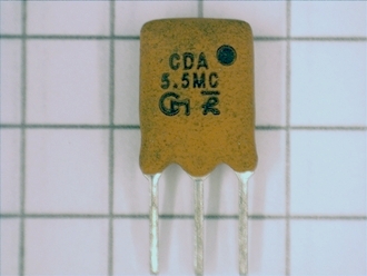
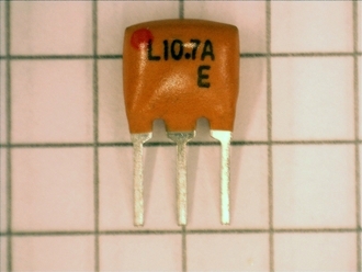
Ceramic Bandpass Filters
A present from the consumer industry :-)
As they are widely used in consumer electronics for IF and RF bandpass filtering, they are made in large quantities and are therefore
available everywhere - at low cost. Some manufacturer even save the money for labelling them. This is some kind of a quick-bleach with a tool to handle
filters of this type with unknown data / performance.
Distinction of sometimes mixed-up technologies
There are three slightly different technologies with specific features. The table below lists them.
Crystal Filters |
1 MHz ... 100 MHz |
very high Q, highly selective, low ageing |
Ceramic Filters |
0.45 MHz ... 10.7 MHz |
small size, low price, highly selective |
SAW Filters |
30 MHz ... 1000 MHz |
compact size, good selectivity |
How does it work ?
In order to see what's inside, we dremel'd open three devices. (one just to see, where not to dremel :-) The other two have been opend
on the front / back side in order to keep half of the stabilising case, as it turned out, that the substrat material is very fragile.


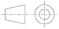
We can see two sections, a left and a right one. The input (pin 1, left) is connected to a metallized area of the substrate. This is the input coupler. In the middle (left picture), we see the coupling from the left resonator to the right resonator. On the right side, we see the output coupler. Looking at the back side, we see some coupling to gnd (in the middle). All couplers are capacitive, as the size does matter and as we have no dc path. The substrat is a piezoelectric ceramics (barium titanate ceramics, leadzirconate-titanate ceramics, etc.) which acts as an electrical-mechanical transducer and as a mechanical resonator. The voltage applied at the input terminal causes the piezoelectric ceramic to vibrate. Depending on the polarization of the piezo-ceramic, several modes of vibration are possible. The table shows the typical vibrating modes, the shapes
and the applicable frequencies of such ceramic resonators.
With the physical dimensions of the ceramic element, the electrode pattern, and the associated mass loading effect
of the electrodes of the above mentioned piezo-electric substrate, the filter characteristics can be set.
Depending on the polarization of the piezo-ceramic, several modes of vibration are possible. The table shows the typical vibrating modes, the shapes
and the applicable frequencies of such ceramic resonators.
With the physical dimensions of the ceramic element, the electrode pattern, and the associated mass loading effect
of the electrodes of the above mentioned piezo-electric substrate, the filter characteristics can be set.
Source: muRata, Ceramic Filter Application Manual.
We can see two sections, a left and a right one. The input (pin 1, left) is connected to a metallized area of the substrate. This is the input coupler. In the middle (left picture), we see the coupling from the left resonator to the right resonator. On the right side, we see the output coupler. Looking at the back side, we see some coupling to gnd (in the middle). All couplers are capacitive, as the size does matter and as we have no dc path. The substrat is a piezoelectric ceramics (barium titanate ceramics, leadzirconate-titanate ceramics, etc.) which acts as an electrical-mechanical transducer and as a mechanical resonator. The voltage applied at the input terminal causes the piezoelectric ceramic to vibrate.
Depending on the polarization of the piezo-ceramic, several modes of vibration are possible. The table shows the typical vibrating modes, the shapes
and the applicable frequencies of such ceramic resonators.
With the physical dimensions of the ceramic element, the electrode pattern, and the associated mass loading effect
of the electrodes of the above mentioned piezo-electric substrate, the filter characteristics can be set.
Source: muRata, Ceramic Filter Application Manual.
Impedance matching
Impedance matching is well known from rf circuit design. There, the goal is to transfer the maximum possible amount of the signal
(which is in the microvolt range). When dealing with ceramic filters, using the correct termination resistors ensures, that the filter
performs maximal. A mismatch will increase the insertion loss, shift the center frequency and increase the ripple. The measurement below
shows a mismatched 10.7 MHz bandpass filter (muRata).
Blue: 50 Ω (too low), black: 330 Ω (nominal), red: 1 kΩ (too high)
Blue: 50 Ω (too low), black: 330 Ω (nominal), red: 1 kΩ (too high)
UMA : Universal Measurement Adapter
This adapter was inspired by the measurement setup given in the datasheet.
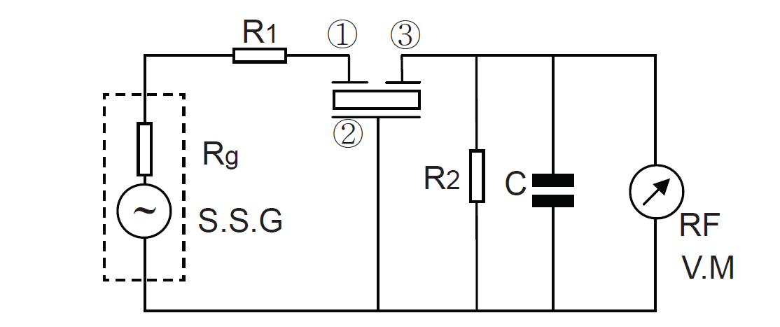
Drawing courtesy of TOKEN ELECTRONICS IND. CO., LTD.
Assuming, that the impedance (of the filter) is always larger than Rg = 50 Ω, we can use a tandem potentiometer with 2 x 1 kΩ for R1 and R2. (In case you want to measure also 450 kHz filters, a tandem potentiomter of 2 kΩ is recommended.) To have symmetrical conditions, R2 consists of the potentiometer and a series 51 Ω resistor. To be able to connect a low impedance measurement instrument like a network analyser, the impedance R2 must be transformed to 50 Ω again. This is done with an opamp. We use the THS3201 from Texas Instruments. (Unity-Gain Bandwidth: 1.8 GHz, Slew Rate: 6700 V/µs)
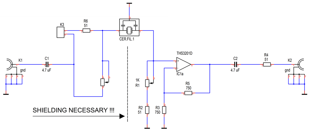
The proposed schematic, bias not shown. K1: Port 1, K2: Port 2 of the NWA.
The opamp acts as impedance transformer, as it has a high impedance input and a low impedance output. The resistor R4 defines the output impedance. The gain has been set to Vu = 2 because the output resistance together with the input impedance of the network analyser form a voltage divider and therefore the overall gain is 1. This can be easily checked, if a bridge instead of the filter is inserted.
After having found the optimum resistance of the unknown filter, the resistance may be measured using K3 with a standard multimeter. (Disconnect the rf source, as it mayst confuse the multimeter) Please also note, that the THS3201 supply should not be larger then ±7.5 V. Current cosumption was 10 mA @ ±5 V.
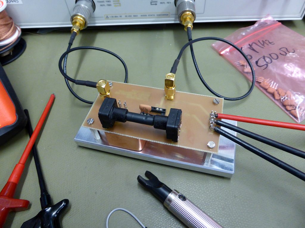
The prototype of the Universal Measurement Adapter
Drawing courtesy of TOKEN ELECTRONICS IND. CO., LTD.
Assuming, that the impedance (of the filter) is always larger than Rg = 50 Ω, we can use a tandem potentiometer with 2 x 1 kΩ for R1 and R2. (In case you want to measure also 450 kHz filters, a tandem potentiomter of 2 kΩ is recommended.) To have symmetrical conditions, R2 consists of the potentiometer and a series 51 Ω resistor. To be able to connect a low impedance measurement instrument like a network analyser, the impedance R2 must be transformed to 50 Ω again. This is done with an opamp. We use the THS3201 from Texas Instruments. (Unity-Gain Bandwidth: 1.8 GHz, Slew Rate: 6700 V/µs)
The proposed schematic, bias not shown. K1: Port 1, K2: Port 2 of the NWA.
The opamp acts as impedance transformer, as it has a high impedance input and a low impedance output. The resistor R4 defines the output impedance. The gain has been set to Vu = 2 because the output resistance together with the input impedance of the network analyser form a voltage divider and therefore the overall gain is 1. This can be easily checked, if a bridge instead of the filter is inserted.
After having found the optimum resistance of the unknown filter, the resistance may be measured using K3 with a standard multimeter. (Disconnect the rf source, as it mayst confuse the multimeter) Please also note, that the THS3201 supply should not be larger then ±7.5 V. Current cosumption was 10 mA @ ±5 V.
The prototype of the Universal Measurement Adapter
UMA : (Self-) Test
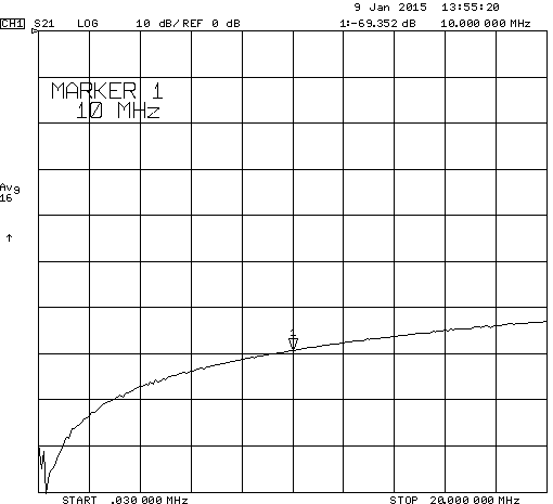
Measurement 1 Crosstalk, no filter is in- serted. Useful to determine the maximum stopband attenuation. This value should not reduce the dynamic range of the NWA significantly. If it is too low, check the shielding. We measure -69 dB @ 10 MHz. BW: 3.7 kHz. |
|
|
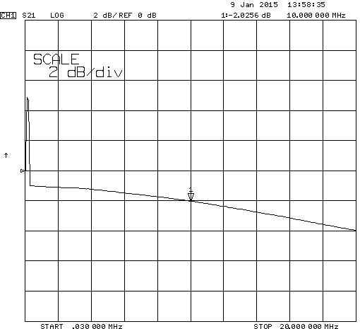
Measurement 2 Frequency response of the amplifier in the adapter. Bridge is inserted. Even so you can calibrate that out, the drop in the amplitude should not be too high in order to maintain a useful s/n ratio. NWA is not calibrated. Resistors set to 1.05 kΩ. |
|
Fazit
The developped measurement adapter shows to be a useful tool, especially in connection with a network analyser. Beeing able to change the impedances
(source and load) continuously and observe the amplitude response is very informative. Depending on the application, it mayst be desireable to use
those ceramic filters on purpose at a different impedance, as it could be observed, that the passband gets flatter (6 MHz filter) or the slope steeper.
You are also able to measure, where the manufacturer stops to measure, as the stopband attenuation is unfavorable. During all measurements,
we saw that different filters are obviously optimised for different goals. (Even if the application was the same !)
Downloads


")
Appendix
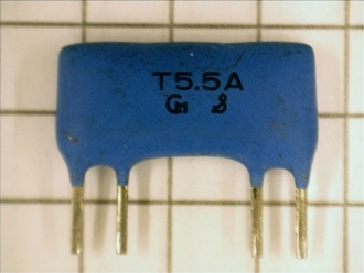
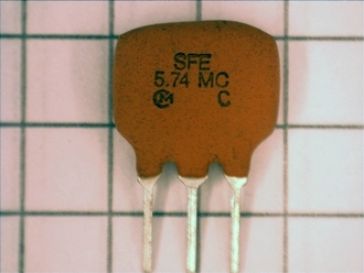
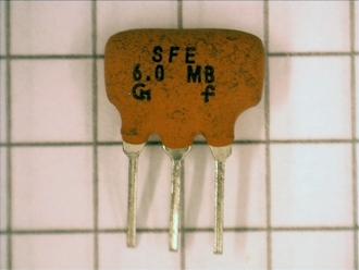
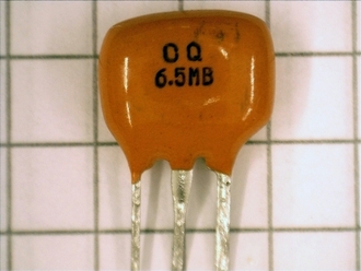
Typical values of some filters. Just to have an idea.
450 kHz |
1 ... 2 kΩ |
SFU/SFZ SERIES, 450–470kHz |
5.5 MHz |
≈ 600 Ω |
4.5-6.5MHz Chip Type SFSKA Series |
6.0 MHz |
≈ 470 Ω |
3.5-6.5MHz Low Profile Type SFSRL Series |
10.7 MHz |
330 Ω |
SFE10.7/SFT10.7/CDA10.7 SERIES |
Hints
In the first version, we used a tandem potentiometer. Due to the parallel alignement of the resistor traces in it,
this formed a coupler, where the coupling could be set by the amout of resistance. Version 2 therefore uses two separate
potentiometers, mechanically coupled and isolated by a shield.
With a tandem potentiometer and no filter, we measured S21: -48 dB at 6 MHz and 0 Ω, increasing with frequency and resistance to about -28 dB (1 kΩ, 6 MHz). Too few to see how a filter performs in the stopband.
With a tandem potentiometer and no filter, we measured S21: -48 dB at 6 MHz and 0 Ω, increasing with frequency and resistance to about -28 dB (1 kΩ, 6 MHz). Too few to see how a filter performs in the stopband.
✈ Share your thoughts
The webmaster does not read these comments regularely. Urgent questions should be send via email.
Ads or links to completely uncorrelated things will be removed.
|
t1 = 7319 d
t2 = 331 ms |
★ ★ ★ Copyright © 2006 - 2026 by changpuak.ch ★ ★ ★
|
|